Wednesday, February 24, 2016

Harman Kardon 250 Stereo Tube Power Amplifier

Harman Kardon 250 Stereo Tube Power Amplifier

03/04/2016 Update*
http://marantzhallo-fi.blogspot.com/2016/03/harman-kardon-250-rectification-close-up.html


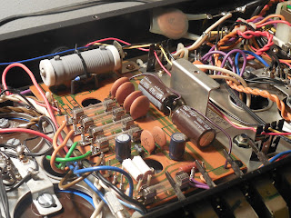
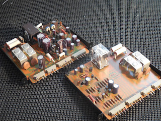
Here we’ve got a vintage-audio members Harman Kardon 250 Tube Power Amplifier. Running of a quad of 6L6 and front end 6CG7 signal gain tubes coupled to 32<tap output transformers.  The 250 amplifier was built with a all copper chassis, something you don’t see very often, or at least under 1K$. The 250 can be ran bridged potentially or as an independent, built 1959 the original tubes were still in place with only a little oxidization occurring on the chassis.  For this rebuild all resistors, capacitors including filtering and multi-section along with a new tube compliment by Electro-Harmonix were selected. 


Power Supply/ Rectification
The first area addressed was the power supply and rectification stages. The rectification consists of tiered silicon diode rectifies and large C13/14 smoothing paper-electrolytic capacitors, these were replaced with built up 100+47MFD/450V Nichicon TVX axial capacitors. The recitifcation stage if examine is kinda unique; in effect its utilizing a 1/2 Wave rectification stage on each side of the C13/C14 smoothing capacitors working out to about 200V+ across each cap in its energize/energize phasing thus working as a voltage double circuit. AC taps consists of a multi-tailed 8(8)MFD/450V paper electrolytic which was replaced with two 10MFD/450V Nichicon TVX capacitors. The large multi-section filter capacitor was disconnected from the chassis to which the grounding is shared. Nichicon low impedance, high temperature (105C) PW capacitors were installed and braced to the chassis in place of the multi-section, the 6.8K and 68 OHM 1W and 2W carbon composite resistors were replaced with flame-proof MOX type 1 and 2W resistors.


 03/04/2016**
In an update blog posted we visited the rectification stage with new Silicon Diodes and 47PF Bypass WIMA films


Moving onto the low signal 6CG7 tubes circuit, the 6CG7 is a twin triode configured miniature packaged tube. Very similar to the 12AU7 layout wise.


Small Signal Process
All carbon composites were removed and replaced with carbon film Vishay resistors. i want to note the about 80% of the carbon composites pulled were grossly off their rating, with an average slew of 20%<.  As has been discussed their are some variations from the actual schematic released (below).  All the 47/100 and 330PF ceramic capacitors were replaced with high grade WIMA pp type film capacitors and all carbon composite resistors replaced with Vishay carbon film resistors.  Each 330/47PF are paralleled. Each balance output pot was cleaned with Caig D5 and adjusted.

SCHEM UPDATES
Plate (#1 of V2 6CG7) R26 56K to 280VAC tap (not) R27(1M)
R30 820OHM parrallel W/ 47PF.


Driver Stage Output
The output stage consists of 2 6L6GC tubes per channel, matched. The 6L6 is a quality power tube typically seen in 25+ watt tube amplifiers, consisting of a beam-pentode large envelope package tied to (<32Ohm) output transformers. The push-pull topography is set to a tetrode-bias configuration capable of rated 25W (the 250 can be ran parallel for up to 50W) at 1%THD.


The large original coupling film capacitors rated .047MFD were upgraded to .22MFD high grade Solen Polypropylene film capacitors with the 180 and 330OHM carbon composites replaced with flame-proof MOX resistors. Below is the 250 getting the balance to equal. no bias concerns need to be addressed as this is a tied cathode tetrode set bias arrangment. Balance is set;


Audio Notizen
Balance (Null) beim widerstand R6 und R21 (100K fur 2.23Vdc)
R6 beim punkten (r4/r7 widerstand)  fur gleich Vdc (2.7V(3.5<))
R21 beim punkten (r19/r22 widerstand fur gleich Vdc (2.7V+)

Audio Notizen Ausgabe (4.5Ohm Precision 10Khz)
Links
7.2VAC (11.52W)
10.4VAC (24.03W)

Recht
7.2VAC

10.4VAC 


10.67<+ max erreicht


Das zoom erreicht 


Wednesday, February 10, 2016

Pioneer SX-1250 Monster Receiver

Pioneer SX-1250 Receiver 


Pioneer SX-1250 Monster Receiver 
Here we have the famous Pioneer SX-1250 Receiver. Built from 1977 to 1979, the 1250 is the predecessor of the larger 1980 and version one of the SX-1280.  The 1250 is a massive unit, with a 62+Lbs chassis, massive heatsink platforms with dual symmetric driver topographies. Each sectional is provided with 44,000 microfarads of filtering! The 1250 continues to impress, with detailed presentation and an overall well-roundedness, these play well with just about everyone.


Power Supply (PSI) AWR-107 PCB
The power supply for the SX-1250 is feed through separated Pformer primary taps for ideal AC separation, feed into dual rectification for each channel via indecent bridge rectifiers filtering at 44,000 microfarads each. The 1250 has a massive Toroidal Pformer, due to their characteristics of high quality toroidal winding after load in resistance and inductance breakdown is almost negligible , due to this factor a MASSIVE current limiting resistor is used tied to a thermistor device (R1 3.3 Ohm 20W!) due to this the PCB and soldering junctions are severally toasted and need to be addressed, because of the surge suppression circuit a 48Vdc Relay is in line with the inline fusing and secondary rectification to shunt in cause of failure or surge.  Another eat caveat of the 1250 PS is the use of rectified DC lamp rails, most 70’s era equipment, even in the top tier still used incandescent AC lamps, DC rails allows for a more stabile illumination and longer bulb life.   


All the radial capacitors were replaced with high temp (105C) long life Panasonic FC’ capacitors, as many of you know I hate axial constructed capacitors, the AWR-107 uses two massive 470/100MFD axial capacitors, these were replaced with radial counterparts using low impedance high temp (105C) variant Nichicon PW’s and fixed to the PCB.

New high grade Nippon filter capacitors were replaced, using 22,000 MFD 100V screw terminated type.


Protection AWM-091 (PSIII) PCB & Stabilizer AWR-106 (PSII) PCB’s
The SX-1250 protection circuit employs the use of three activations in 3 stages, DC deviation protection for your speakers, DC overload saturation of the power transistor devices and finally On/Off cycle muting, which is very similar to the soft start integration. A MY-4 DPDT 24Dc relay is coupled with the output stage devices, which was replaced with a low Noise Omron MY4. The overload protection is designed in series of resistors who’s potential dictates the cutoff point, inline with the relay drive circuit and is expelled via a cut off point, as with the excessive current flow turning on the Q1 flowing through D3 which is then shunted via C1 capacitor.  All the electrolytics were replaced with either low impedance, high temp variant PWs or Panasonic high temp FC’s, differential pick up transistors on the stabilizer updated right angle potentiometers installed.  On the Protection I should note that the 945 class BJT’s tend to fail or become open during loads causing relay malfunctions, a second attempt on this PCB replaced all BJT,s with 1845, 992 low signal devices and 2690 TO-tabbed devices and updated diodes to all 1n4148 type.  Due to the large limiter resistors and its location the stabilizer PCB suffers excessive heat issues, all solder junctions must be at minimal reflowed on this PCB.


Power Amplifier AWH-048 PCB
One of the most important stages of the receiver short of the PS in my opinion, so I always takes special care here to optimize what we can.  Designed around a classic a/b configuration the x1250 encompasses a 1st order differential pair gain stage tied to a constant current mirror design which mutually phases signal for a more stabile drive via Q3-4 und Q5/6 through a/b biasing resulting in a PP bias scheme.  3rd order drive is comprised of a tiered complimentary  darlington arrangement via BJT’s through to outputs. This is a vastly different circuit employees versus the 1280.


The differential pair transistors were updated to matched he KSA992 transistors along with Q11 to low signal KSC1845 transistors, 2nd order were updated to 2690/1220A transistors and 3order drivers to MJE15033/32 50W250V devices with new thermal compound and mica insulators. All electrolytic were updated to low impedance high temp (105C) Nichicon PW and audio grade FG’ Nichicon (.22MFD), new high grade Panasonic ECW polypropylenes (1MFD) and right angle pots. Pin connectors were all reflowed do to the vertical stress of the PCB.  TO-3 banks were pulled and re-greased as well. 


Audio Notizen
Bias beim punkten #7 und #19 fur 100mV links und recht

Phono/RIAA AWF-021 & Filter Amp AWM-089 PCB’s
The AWF-021 circuit uses a tied emitter differential transistor group for 1st order gain while employing a SEPP )(single ended pp) complimentary circuit for voltage gain drive, high grade polystyrene and precision 1>% resistors results in incredible noise reduction and almost no discernible deviation (>.2dB)  All the electrolytic were replaced audio grade Nichicon KA and low impedance Nichicon PW capacitors, differential pair updated and original mylar upgraded to high grade Panasonic ECW polypropylene film capacitors.


The Filter Amp assembly is comprised of a 2 tied capacitor/resistor emitter NFB circuit resulting in apparently sharper filter response. The AWM-089 originally hosted a plethora of tantalum capacitors, tantalum capacitors are considered poor due to their potential microphonic and poor audio characteristics, they also do not uniformly conform and tend to fail rather catastrophically, these were all replaced with low impedance Nichicon PW capacitors. Its important at this stage to pull the remaining switching assemblies so you can properly clean everything. 


Flat Amp AWG-042 & Control Amp AWG-041 
The pre-amp uses a complimentary set of FET transistors tied to a direct coupled drive stage. Control assembly AWG-041 is a two stage NFB circuit designed to allow low frequency attenuations (ultraslow and to extreme). One nice point on the SX1250 is the use of extra shielding on the tone amp PCB, this is in proximity to the RF stage gang capacitor and with open framed potentiometers is makes a significant difference in noise reduction.  All tantalum capacitors on the flat were removed and replaced with low impedance PWs, all others were replaced with low impedance PW and audio grade Nichicon KA capacitors. All 1 MFD films were replaced with high quality Panasonic ECW polypropylene film capacitors.


Control Amp AWG-041 


Tuner Assembly AWE-068
The SX-1250 has an incredible FM/AM sectional, with a highly sensitive 5-gang FM tuning capacitor and 3 gang AM, the fm is driven from a dual stage gain circuit while employing an array of MOS/FET and AM IC gain stages (HA1138). Both tuning capacitors were carefully cleaned and treated, all electrlyotics over .1MFD were replaced with high temp (105C) low impedance Nichicon PW type while .1> were replaced with stacked WIMA film capacitors (whites). The nice addition is the shielding used in front end chassis, all RIAA and RF stages have separated shielding.


Audio Notizen

1Khz @ 4.5 Ohm
Links
4.024
13.25 (39.01W


Recht
4.029
13.01 (37.61W


10Khz @ 4.5 Ohm
Links
5.10 (5.78W
26.06 (150W PICTURED & CLOSE UP WAVE


Recht
5.08 (5.73W
25.51 (144W PICTURED & CLOSE UP WAVE


Wednesday, February 3, 2016

Harman Kardon 430 Dual Power Receiver

Harman Kardon 430 Dual Power Receiver 


Thought I’d do a quick write up on a nice H&K 430 dual powered receiver we received in recently. 
Very similar to the 330 and 730 topographies, the 430 is rated at a minimal 25W/ch, the biggest retraction from the 730 is the lack of pre-out/main in jumpers. 


Power Supply & Dual Rectifications
The integrated separated power supplies is a neat feature of this H&K series. Quite a bit different than most supplies, the only issue Ive noted is one transformer is delivering a current draw of 1.25A for the bulbs running it a little hotter than the other.  Each rectification PCB A & B had the large electrolytic replaced with 330<MFD low impedance, high temp (105C) Nichicon PW’s along with the SIB01-02 updated to a ultra fast diode and 1/25V/1/13V diodes updates. 


Driver PCB
The symmetric driver pcbs has a mounted heatsink to the PCB hosting the TO-3 output device bank, new MICA and compound was applied here along with pin junctions reflowed. The original 2W emitter resistors were replaced with .47 5W wire wounds for better dissipation and pigtailed for future bias adjustments. New precision Bourns bias potentiometers were installed, notate the common wiper configuration. 1st order differential pair transistors were replaced with HFe matched 1845 BJ-transistors along with Q421/422 which is a failure prone 2c458 TO-92 BJ-Transistors, these are commonly found in the RIAA stage of Marantz and in pre-amp stages for low signal gain drivers, very problematic and noise prone. Electrolytic were replaced with low impedance, high reliability Nichicon PW and .22/250V film updates to a polypropylene type.  D407/408 diodes were updated to ultra fast 4005 type.


Bias Notizen
Links und Recht beim emitterwiderstand R430 und R429 beim VR402/1 fur 25mV


Tone/RIAA(EQ)
All the electrolytic within the RIAA and tone stages were replaced with low impedance, high reliability Nichicon PW and audio grade Elna Silmic II, the RIAA stage small MFD capacitors were replaced with high quality WIMA polypropylene type film capacitors with a 2mm footprint. The Tone control can be tricky to get at, make sure you pull the PCB from the chassis as this is the best angle to clean all the potentiometers and switching controls. Updated from the early H&K receivers the 2SC1344 PNP BJ-transistor was used exclusively vs the 458BJT. 


RF Stages

Like many RF stages we do, all the tantalums were removed and replaced along with electrolytic dielectric capacitors to Nichicon PW low impedance capacitors.  Special care was taken to clean the shaft and tuning capacitors along with a new replaced stereo indicator.